
Patterning

---Au-500-A---20-pkg_2")
Shadow Masking
- We design stainless steel shadow masks to pattern thin films during deposition.
- We will convert any drawing (CAD, JPEG, TIFF, etc.) into the appropriate format for mask fabrication.
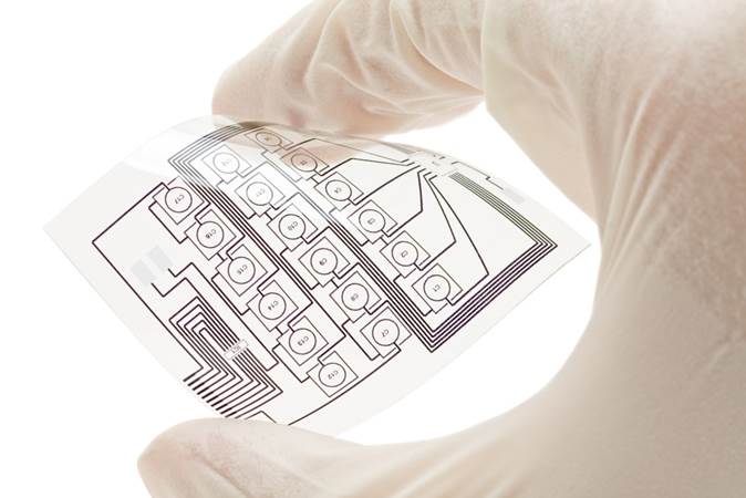
Photolithography
- High resolution patterning over large areas is achieved using a combination of photo-lithography and lift-off or chemical etching.
- Photo masks are designed in-house according to customer specifications.
FIB Milling
- Ion milling and micromachining can be done in-situ during SEM imaging.
- Highest resolution patterning can be achieved using in-situ SEM lithography.
Reactive Ion Etching (RIE)
- Many materials can be patterned by reactive ion plasma etching using patterned photoresist as a mask.
Looking for custom substrates or coatings?
We're here to help! Please fill out our Request a Quote form.